- 您现在的位置:买卖IC网 > Sheet目录3887 > PIC16F872T-E/SO (Microchip Technology)IC MCU CMOS 20MHZ 2K FLSH 28SOIC
155
8048C–AVR–02/12
ATtiny43U
loading the Write EEPROM Memory Page Instruction with the 4 MSB of the address.
When using EEPROM page access only byte locations loaded with the Load EEPROM
Memory Page instruction is altered. The remaining locations remain unchanged. If poll-
ing (RDY/BSY) is not used, the used must wait at least t
WD_EEPROM before issuing the
next page (See Table 19-15 on page 155). In a chip erased device, no 0xFF in the data
file(s) need to be programmed.
6.
Any memory location can be verified by using the Read instruction which returns the
content at the selected address at serial output MISO.
7.
At the end of the programming session, RESET can be set high to commence normal
operation.
8.
Power-off sequence (if needed):
Set RESET to “1”.
Turn V
CC power off.
19.7.2
Serial Programming Instruction set
Table 19-16 and Figure 19-8 on page 157 describes the Instruction set.
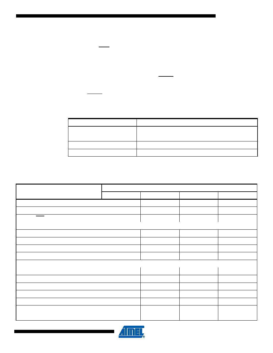
Table 19-15. Minimum Wait Delay Before Writing the Next Flash or EEPROM Location
Symbol
Minimum Wait Delay
tWD_FLASH
4.5 ms
tWD_EEPROM
4.0 ms
t
WD_ERASE
9.0 ms
tWD_FUSE
4.5 ms
Table 19-16. Serial Programming Instruction Set
Instruction/Operation(1)
Instruction Format
Byte 1
Byte 2
Byte 3
Byte4
Programming Enable
$AC
$53
$00
Chip Erase (Program Memory/EEPROM)
$AC
$80
$00
Poll RDY/BSY
$F0
$00
data byte out
Load Instructions
Load Extended Address byte
$4D
$00
Extended adr
$00
Load Program Memory Page, High byte
$48
adr MSB
adr LSB
high data byte in
Load Program Memory Page, Low byte
$40
adr MSB
adr LSB
low data byte in
Load EEPROM Memory Page (page access)
$C1
$00
adr LSB
data byte in
Read Instructions
Read Program Memory, High byte
$28
adr MSB
adr LSB
high data byte out
Read Program Memory, Low byte
$20
adr MSB
adr LSB
low data byte out
Read EEPROM Memory
$A0
$00
adr LSB
data byte out
Read Lock bits
$58
$00
data byte out
Read Signature Byte
$30
$00
adr LSB
data byte out
Read Fuse bits
$50
$00
data byte out
Read Fuse High bits
$58
$08
$00
data byte out
发布紧急采购,3分钟左右您将得到回复。
相关PDF资料
PIC16F727-E/P
IC PIC MCU FLASH 8KX14 40-DIP
PIC16F871T-E/PT
IC MCU CMOS 20MHZ 2K FLSH 44TQFP
PIC16F871T-E/L
IC MCU CMOS 20MHZ 2K FLSH 44PLCC
PIC16F871-E/PT
IC MCU CMOS 20MHZ 2K FLSH 44TQFP
PIC16F871-E/L
IC MCU CMOS 20MHZ 2K FLSH 44PLCC
PIC16F870T-E/SS
IC MCU CMOS 20MHZ 2K FLSH 28SSOP
PIC16F870T-E/SO
IC MCU CMOS 20MHZ 2K FLSH 28SOIC
PIC16F84AT-20E/SS
IC MCU CMOS 20MHZ 1K FLSH 20SSOP
相关代理商/技术参数
PIC16F872T-E/SS
功能描述:8位微控制器 -MCU 3.5KB 128 RAM 22 I/O RoHS:否 制造商:Silicon Labs 核心:8051 处理器系列:C8051F39x 数据总线宽度:8 bit 最大时钟频率:50 MHz 程序存储器大小:16 KB 数据 RAM 大小:1 KB 片上 ADC:Yes 工作电源电压:1.8 V to 3.6 V 工作温度范围:- 40 C to + 105 C 封装 / 箱体:QFN-20 安装风格:SMD/SMT
PIC16F872T-I/SO
功能描述:8位微控制器 -MCU 3.5KB 128 RAM 22 I/O RoHS:否 制造商:Silicon Labs 核心:8051 处理器系列:C8051F39x 数据总线宽度:8 bit 最大时钟频率:50 MHz 程序存储器大小:16 KB 数据 RAM 大小:1 KB 片上 ADC:Yes 工作电源电压:1.8 V to 3.6 V 工作温度范围:- 40 C to + 105 C 封装 / 箱体:QFN-20 安装风格:SMD/SMT
PIC16F872T-I/SS
功能描述:8位微控制器 -MCU 3.5KB 128 RAM 22 I/O RoHS:否 制造商:Silicon Labs 核心:8051 处理器系列:C8051F39x 数据总线宽度:8 bit 最大时钟频率:50 MHz 程序存储器大小:16 KB 数据 RAM 大小:1 KB 片上 ADC:Yes 工作电源电压:1.8 V to 3.6 V 工作温度范围:- 40 C to + 105 C 封装 / 箱体:QFN-20 安装风格:SMD/SMT
PIC16F872T-I/SS033
制造商:Microchip Technology Inc 功能描述:
PIC16F873-04/SO
功能描述:8位微控制器 -MCU 7KB 192 RAM 22 I/O RoHS:否 制造商:Silicon Labs 核心:8051 处理器系列:C8051F39x 数据总线宽度:8 bit 最大时钟频率:50 MHz 程序存储器大小:16 KB 数据 RAM 大小:1 KB 片上 ADC:Yes 工作电源电压:1.8 V to 3.6 V 工作温度范围:- 40 C to + 105 C 封装 / 箱体:QFN-20 安装风格:SMD/SMT
PIC16F873-04/SO
制造商:Microchip Technology Inc 功能描述:8BIT FLASH MCU SMD 16F873 SOIC28
PIC16F873-04/SP
功能描述:8位微控制器 -MCU 7KB 192 RAM 22 I/O RoHS:否 制造商:Silicon Labs 核心:8051 处理器系列:C8051F39x 数据总线宽度:8 bit 最大时钟频率:50 MHz 程序存储器大小:16 KB 数据 RAM 大小:1 KB 片上 ADC:Yes 工作电源电压:1.8 V to 3.6 V 工作温度范围:- 40 C to + 105 C 封装 / 箱体:QFN-20 安装风格:SMD/SMT
PIC16F873-04/SP
制造商:Microchip Technology Inc 功能描述:IC 8BIT FLASH MCU 16F873 SDIL28